Explore our premium line of integrated signal interconnect components, mechanical cages, and optical transceivers designed for high-performance networks.
Analyzing the shift toward hyperscale network architectures, AI workloads, and optical engine development.
The global telecommunications and datacom sectors are undergoing an unprecedented technological expansion. Driven by computational workloads such as Generative Artificial Intelligence (AI), Machine Learning (ML) clusters, Internet of Things (IoT) ecosystems, and global 5G/6G deployments, the demand for optical transceivers has surged. Modern optical transceivers serve as the critical bridge transforming electrical data streams into high-speed light paths, enabling low-latency communication across fiber optic links.
As data centers migrate from legacy 100G configurations to 400G, 800G, and 1.6T physical layers, optical transceivers must incorporate advanced modulation formats like PAM4 and coherent detection to maximize spectral efficiency.
Power density remains a major constraint in cloud facilities. System designers require transceivers with extremely low power consumption (Watts per Gigabyte) to keep overall server farm cooling costs and infrastructure demands in check.
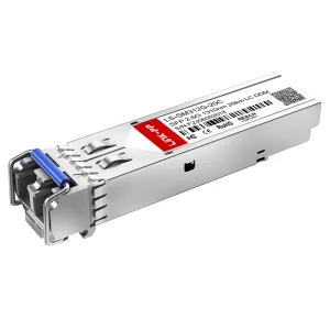
Multi-Source Agreements (MSAs) establish standards for mechanical form factors (SFP, SFP28, QSFP28, QSFP-DD, OSFP) and electrical interfaces. Adhering to these standards ensures hardware interoperability across global networks.
"The transition towards optical computing interconnects demands absolute precision in electro-optical alignment. At the industrial level, even a sub-micron deviation in the placement of the transmitter optical sub-assembly (TOSA) can lead to devastating packet loss and optical back-reflection."
Moreover, the integration of silicon photonics has transitioned from a theoretical research topic into a standard design pattern for high-volume manufacturing. By leveraging existing semiconductor fabrication nodes, silicon photonics allows for co-packaging lasers and optical components directly onto silicon dies. This technological shift addresses the physical limitations of copper connections, lowering transmission loss and ensuring high reliability in enterprise datacenters.
Introducing our state-of-the-art optical transceiver manufacturing facility and core technical focus.
OptiLinker Optoelectronics Co., Ltd. (OptiLinker) is a professional optical transceiver manufacturer and solution provider operating under the registered brand OptiLinker (www.optilinkertrans.com). Established in 2016, OptiLinker is built on a foundation of over 12 years of industry experience and approximately 8 years of international export experience, engineering optical communication modules for global telecom operators, enterprise networks, and cloud datacenters.
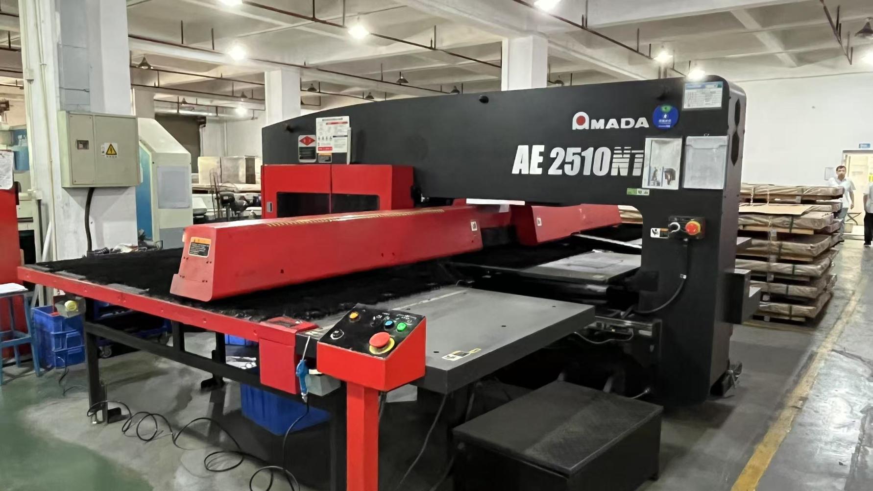
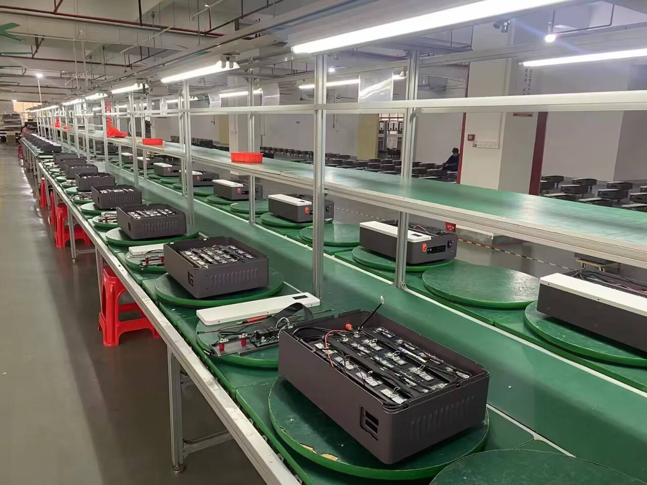
OptiLinker's operations are situated in a modern precision production facility. Spanning a specialized layout of approximately 320㎡, this facility functions as a high-density, dust-free optical micro-assembly cleanroom. Having a highly optimized workspace allows our engineering teams to maintain micro-environment controls for relative humidity, ambient temperature, and particulate filtration. This is crucial for optical alignment procedures where micro-dust can compromise laser components.
We enforce a rigorous quality control program managed by 35 dedicated QC professionals. The pipeline includes 100% incoming material inspections, Automated Optical Inspection (AOI), Bit Error Rate (BER) testing, eye diagram analysis, and environmental stress screening (temperature cycling).
Supported by a team of 60 optical engineers, we offer customization services for wavelength tuning (CWDM/DWDM), transmission range, EEPROM compatibility coding for switches, and proprietary firmware modifications.
We collaborate with a robust global network of approximately 850 supply chain partners, enabling stable manufacturing outputs. In the past year alone, OptiLinker introduced 120 new products to meet changing demand.
OptiLinker achieved an annual export revenue of approximately USD 12 million last year. Our market footprint spans across North America, Europe, Southeast Asia, and the Middle East, serving telecommunications operators, hyperscale data centers, network integrators, and OEMs who require highly reliable and cost-effective fiber optical hardware solutions.
How localization, raw material access, and manufacturing engineering translate to cost and design speed advantages.
China's Yangtze River Delta and Pearl River Delta regions represent the world's most concentrated optical communication supply hubs. By locating manufacturing operations within this industrial ecosystem, OptiLinker provides distinct commercial advantages for global buyers:
This ecosystem enables OptiLinker to quickly scale production for high-volume orders while maintaining the flexibility required to execute low-volume, highly customized production runs. Rather than facing long supply chains for specialty connectors, waveguides, or specialized firmware, OptiLinker consolidates these components locally to deliver short lead times.
Our products are engineered to function across varied operational environments, from dry-room server farms to industrial edge nodes.
Engineered for spine-leaf architectures where switch-to-switch links require high density and performance. OptiLinker transceivers support 40G, 100G, and next-gen standards over single-mode (SMF) and multi-mode (MMF) fiber paths.
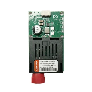
Supporting metropolitan networks and long-haul transport. Our DWDM, CWDM, and bidirectional (BiDi) transceivers utilize single-fiber optical interfaces to maximize existing fiber plant investments over distances up to 80km.
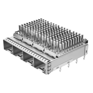
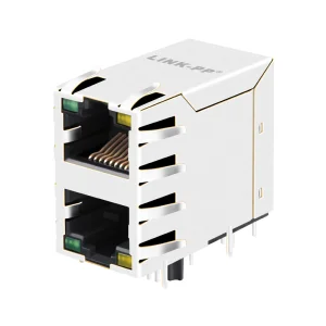
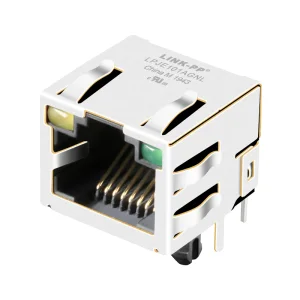
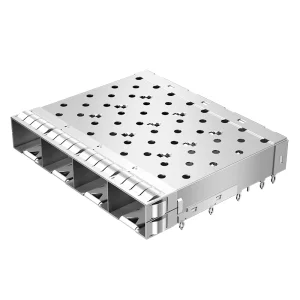
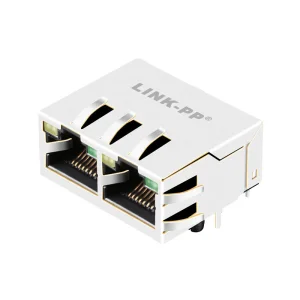
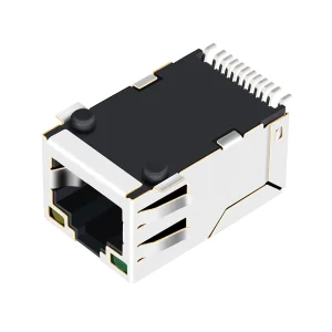
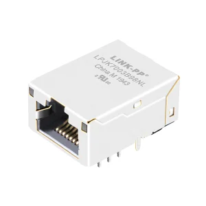
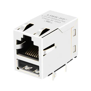
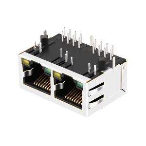
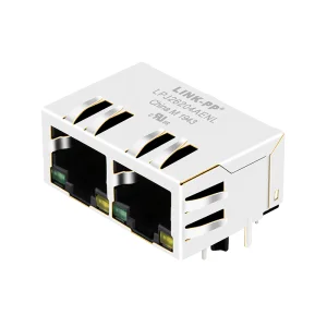
For environments with high electromagnetic interference (EMI). We provide fully shielded RJ45 magnetic connectors, filtered jacks, and rugged SFP cages designed to maintain high signal integrity in factory and transport hubs.
Navigating the next generation of physical layer transceivers and high-density networking designs.
As network bandwidth requirements scale, conventional optical transceiver design is reaching physical limitations. Energy loss at high frequencies restricts standard copper PCB traces, driving the industry to explore alternative interconnect architectures:
LPO transceivers remove the Digital Signal Processor (DSP) from the optical module, relying on the host ASIC's high-performance serializer/deserializer (SerDes) to drive the optical modulator directly. Removing the DSP significantly reduces power consumption (up to 50% per module) and lowers latency, making LPO an attractive design option for short-reach AI cluster interconnects.
CPO replaces traditional pluggable form factors by mounting the optical engines directly onto the same organic substrate as the network switch ASIC. This layout minimizes copper trace lengths, reducing signal attenuation and power consumption. While implementation remains complex due to serviceability and laser reliability concerns, CPO is positioned to serve as a key technology for switch bandwidths exceeding 51.2 Tbps.
By using standard silicon manufacturing lines, Silicon Photonics integrates lasers, optical waveguides, modulators, and photodetectors directly onto a silicon die. This integration yields more compact structures, cleaner signal paths, and improved scalability, allowing manufacturers to optimize the cost-per-gigabit for high-volume 400G and 800G modules.
Our manufacturing processes integrate high-precision assembly lines and dedicated optical validation labs to verify every transceiver before shipment.
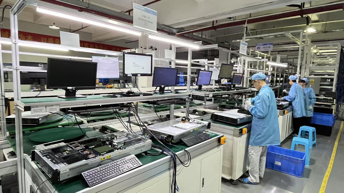
OptiLinker’s quality control protocol is structured to verify that every module meets or exceeds MSA specifications. Optical validation includes:
Technical clarifications and procurement guidance for network engineers and purchasing professionals.
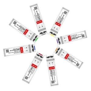
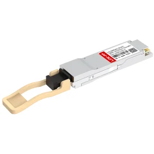
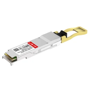
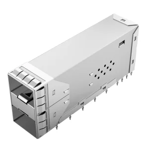
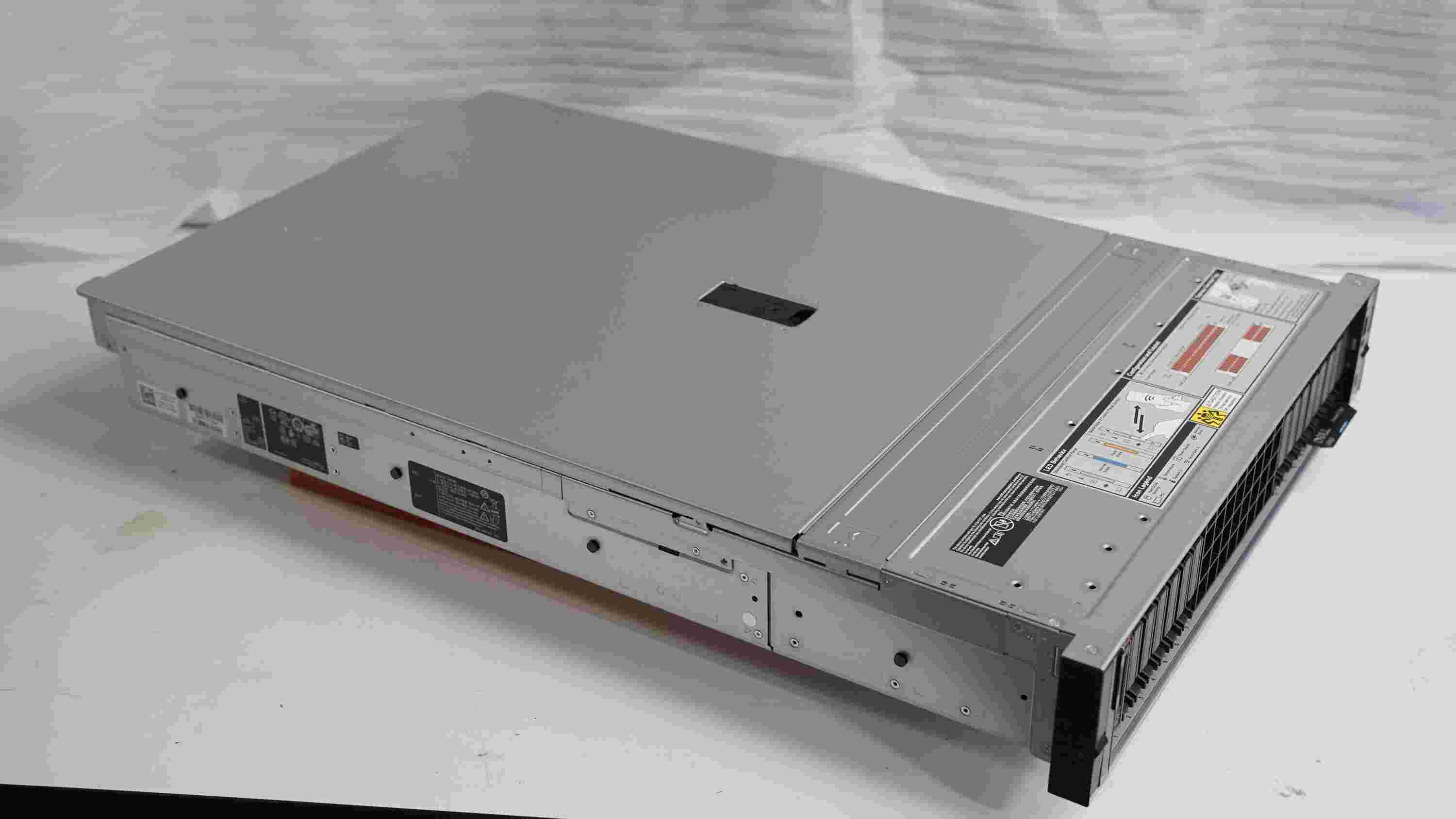
High-performance pluggable optical transceivers and shielding options engineered for enterprise networks and telecoms.